
·For power analysis, each cell’s power dissipation has been characterized in the library (.lib) file. For leakage power, the EDA tool simply adds up the leakage power of each cell. (Note: Leakage power is usually state dependent) For dynamic power, the EDA tool either estimates net capacitance before P&R or calculates net capacitance after P&R. The designer has to provide the toggle rate. This can be based on educated guess, experience, simulation, or emulation.
21-08-2025
What is LVS and Inputs required? Difference between schematic and layout views? Is it a functional check?
oLVS (Layout Versus Schematic): A critical physical verification process that compares the electrical circuit extracted from the physical layout database (e.g., GDSII, OASIS) against the intended circuit described by the source schematic netlist (e.g., SPICE or Verilog netlist).
- Inputs:
- Layout Database: The physical layout design file (GDSII, OASIS)
- Source Netlist: The “golden” netlist representing the intended circuit schematic (e.g., SPICE netlist for custom designs, Verilog netlist for digital designs).
- Rule Deck: Provided by the foundry, this file tells the LVS tool how to identify devices (transistors, resistors, capacitors, diodes) from the layout layers, how to determine connectivity, and how to extract parameters (like W/L for transistors).
- Configuration/Setup Files: Files to control the LVS run, specify top cells, map power/ground names, define device properties to compare, set tolerances, etc.
- Schematic View vs. Layout View (in LVS context):
Schematic View: Circuit from Golden netlist.
21-08-2025
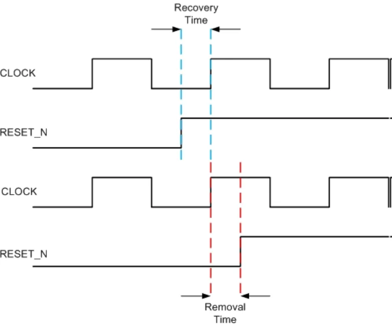
What is recovery and removal time?
oRecovery time is the minimum amount of time required between the release of an asynchronous signal from the active state to the next active clock edge.
Removal time specifies the minimum amount of time between an active clock edge and the release of an asynchronous control signal.
The following diagram illustrates recovery and removal times for an active low reset signal (RESET_N) and positive-edge triggered CLOCK
21-08-2025
What is temperature inversion?
oTemperature Inversion effect is seen at lower technology nodes (28nm and below), where cell delay is inversely proportional to the temperature. This is mainly because of reduced supply voltage at lower nodes.
- Cell delay depends on carrier mobility and threshold voltage of transistor. Both mobility and threshold voltage inversely proportional to the temperature.
- At higher nodes, due to high supply voltage, effect of mobility is dominant over threshold voltage on cell delay. So, As temperature increases, mobility decreasesand cell delay increases.
- While at lower nodes, as supply voltage is reducing, effect of threshold voltage is dominant on cell delay compared to mobility. So, As temperature increases, threshold voltage decreases and cell delay decreases
21-08-2025
What is the difference between cworst/rcworst and C / RC corners? Why do we need to consider different RC corners?
o Traditional Corners (Simplified View - often just called C corners initially): Used for short nets where resistance can be ignored or very less.
Cworst (Maximum Capacitance, Cmax): Models process variations that maximize interconnect capacitance (e.g., wider wires, thicker metal, smaller spacing, higher dielectric constant). Often assumes minimum resistance for these conditions (though not always explicitly linked). Used primarily for setup timing analysis (longest path delay).
Cbest (Minimum Capacitance, Cmin): Models process variations that minimize interconnect capacitance (e.g., narrower wires, thinner metal, larger spacing, lower dielectric constant). Often assumes maximum resistance. Used primarily for hold timing analysis (shortest path delay).
21-08-2025
What is the difference between LVS netlist and PT (Primetime) netlist?
oNetlist used for LVS is PG netlist, meaning it has all PG related components, physical only cells etc. Netlist used for PT has cells required for functionality.