General-Concepts Interview Questions

What are the things needed to be taken from sub-blocks to the main block? How do you take logical information of sub-blocks?

oLogical View (Timing Model - .lib or .db**):**

  • Provides the timing characteristics of the sub-block’s input/output pins (setup/hold times, clock-to-output delays, internal path delays)
  • Defines cell functions (if it’s a soft macro with standard cells) or overall block function.
  • Needed for top-level STA and synthesis (if the sub-block is a soft/firm macro).
  • Physical View (Abstract Layout Model - LEF):
  • .lef file of Hard Macro or soft macro/sub blocks.
  • Defines the physical footprint (width, height), pin locations, pin layers, metal blockages (OBS layers) within the sub-block.
  • Constraint View (SDC partial/interface):
  • Interface timing constraints for the sub-block’s pins (e.g., specific false paths or multicycle paths internal to the IP that the top level should be aware of, or constraints on its I/O pins).
  • UPF and GDS for merging at last to get complete top-level GDS.
What inputs are needed at CTS for sub-blocks?

o The top-level SDC must correctly define the clocks reaching the input clock ports of the sub-blocks.

If a sub-block generates clocks that are used by other blocks or the top level, these generated clocks must also be properly defined (e.g., using create_generated_clock sourced from a sub-block’s output pin).

  • Sub-Block Timing Model (.lib**) and Physical Abstract (LEF):**
  • CTS Exceptions for Sub-Block Pins:

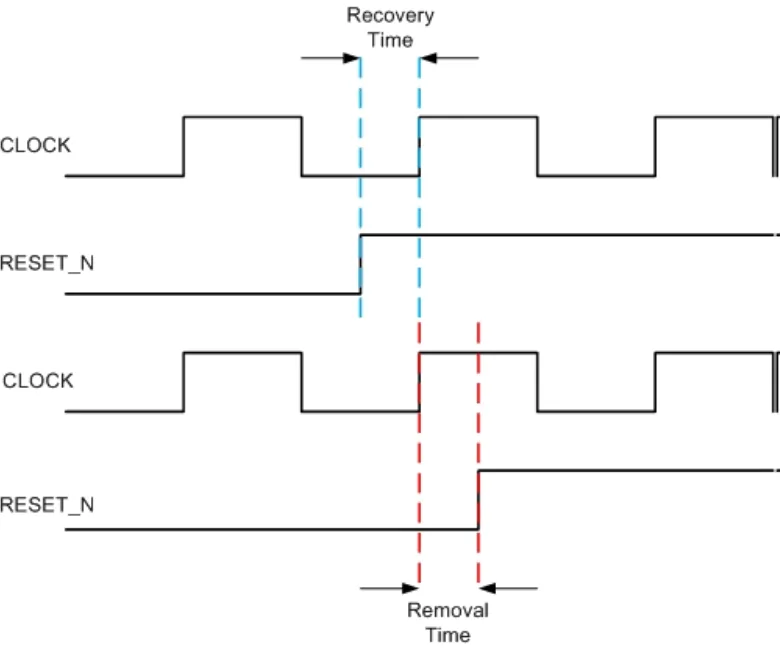
What is recovery and removal time?

oRecovery time is the minimum amount of time required between the release of an asynchronous signal from the active state to the next active clock edge.

Removal time specifies the minimum amount of time between an active clock edge and the release of an asynchronous control signal.

The following diagram illustrates recovery and removal times for an active low reset signal (RESET_N) and positive-edge triggered CLOCK

What is temperature inversion?

oTemperature Inversion effect is seen at lower technology nodes (28nm and below), where cell delay is inversely proportional to the temperature. This is mainly because of reduced supply voltage at lower nodes.

  • Cell delay depends on carrier mobility and threshold voltage of transistor. Both mobility and threshold voltage inversely proportional to the temperature.
  • At higher nodes, due to high supply voltage, effect of mobility is dominant over threshold voltage on cell delay. So, As temperature increases, mobility decreasesand cell delay increases.
  • While at lower nodes, as supply voltage is reducing, effect of threshold voltage is dominant on cell delay compared to mobility. So, As temperature increases, threshold voltage decreases and cell delay decreases

What is the difference between cworst/rcworst and C / RC corners? Why do we need to consider different RC corners?

o Traditional Corners (Simplified View - often just called C corners initially): Used for short nets where resistance can be ignored or very less.

Cworst (Maximum Capacitance, Cmax): Models process variations that maximize interconnect capacitance (e.g., wider wires, thicker metal, smaller spacing, higher dielectric constant). Often assumes minimum resistance for these conditions (though not always explicitly linked). Used primarily for setup timing analysis (longest path delay).

Cbest (Minimum Capacitance, Cmin): Models process variations that minimize interconnect capacitance (e.g., narrower wires, thinner metal, larger spacing, lower dielectric constant). Often assumes maximum resistance. Used primarily for hold timing analysis (shortest path delay).

What is the significance of the Global skew?

  • CTS tools on global skew to start implementing clock tree. The idea is that minimizing the global skew will automatically minimize the local skew as global skew is the upper bound of local skew.
  • Global skew balancing attempts to make the propagated clock timing match the ideal mode clock timing by balancing the insertion delay (clock latency) between all sinks.
  • If you are working on a block and it is a full chip clock domain, the global skew will make effect at full chip timing for global clock balance. You need to meet the latency &. skew requirements for chip timing close.