CTS Interview Questions

Is moving to a higher layer for clock always helpful in reducing delay?

o Moving to a higher layer is not always helpful in reducing delay. It’s a trade-off.

  • Resistance (R): Higher layers have thicker wires, which decreases resistance. This part helps reduce delay (R×C).
  • Capacitance (C): While the area capacitance to the layers below might decrease due to greater distance, the fringe and coupling capacitance can increase because the wires are taller and have more surface area on their sides.

Conclusion: For very long nets, the benefit of lower resistance dominates, and using higher layers is helpful. For shorter nets, the increased capacitance can negate the benefit of lower resistance, potentially even increasing the total delay.
Pros and cons of H-tree? Advantage of using both buffers and inverters?

o H-Tree:

Advantages:

Zero Skew (Ideal): Theoretically capable of achieving zero skew if sinks are perfectly distributed and the tree is perfectly balanced.

Symmetric Structure: Predictable and regular routing pattern.

Disadvantages:

Impractical for Real Designs: Assumes uniform sink distribution, which rarely occurs. Blockages and routing obstacles disrupt the ideal structure.

High Insertion Delay: Can lead to long paths from the root to sinks.

Resource Intensive: Can consume significant routing area, especially on preferred layers.

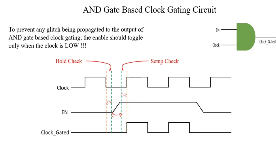
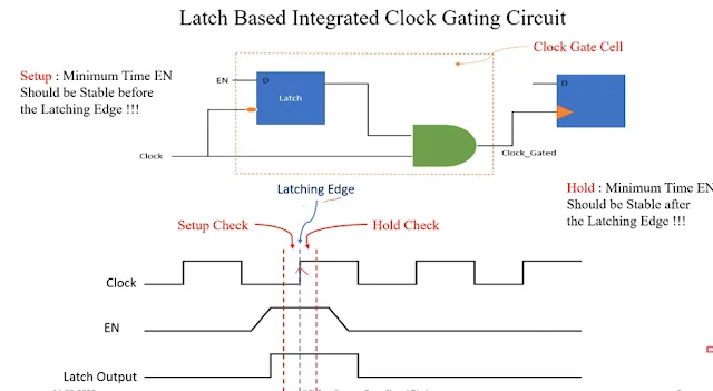
What are clock gating checks? Why do we do them?

Clock Gating Checks: setup and hold timing checks applied to the enable signal of Integrated Clock Gating (ICG) cells.

Prevent Glitches: The primary reason is to ensure the output of the ICG cell (the gated clock) is clean and free from glitches or runt pulses. Glitches can cause flip-flops downstream to capture incorrect data or enter metastable states.

Reliable Low Power: Ensuring the checks pass guarantees the gating works reliably, achieving the intended power reduction without causing functional errors.

What are inputs required to star CTS?

  • Placement Database: The design database after placement is complete, containing the locations of all standard cells (including clock sinks like flip-flops and clock gates) and macros. – it covers Timing lib. Tech lef, std cell lef, SDC etc.

CTS Specification File .ctstch**,** .cts_spec**,** This file (or equivalent tool settings) provides detailed instructions for building the clock tree:

  • Target Skew: Maximum acceptable skew between sinks in the same clock domain or skew group.
  • Target Max/Min Latency: Desired range for insertion delay.
  • Target Max Transition: Maximum allowed transition time for clock nets.
  • Buffer/Inverter List: Specifies the list of buffers and inverters the tool is allowed to use for building the tree (often restricts to specific drive strengths or balanced cells).
  • DRC Constraints: Max capacitance, max fanout limits specifically for clock nets.
  • NDR (Non-Default Rules): Specifies special routing rules (e.g., double width, double spacing, shielding) to be used for clock nets to improve signal integrity and reliability.
  • Routing Layers: Preferred top and bottom metal layers for clock routing.
  • Clock Tree Exceptions: Defines pins to be treated specially:
    • Stop/Sink Pins (Default): Normal clock endpoints to be balanced.
    • Exclude Pins: Excluded from skew/latency balancing but still receive the clock and DRV fixing (e.g., output ports, Multiplexer select pin )
    • Ignore Pins: Completely ignored by CTS balancing and DRC fixing (e.g., non-clock pins driven by clocks, test pins).
    • Float Pins: Similar to Exclude pins but allow specifying a pin delay range for balancing (used for macro models).
    • Non-stop pins: trace through the endpoints that are normally considered as endpoints of the clock tree. Ex, The clock pin of sequential cells driving generated clock are implicit non-stop pins. Clock pin of ICG.
  • Skew Groups: Defines groups of sinks that should be balanced together, potentially with different skew targets than other groups.
  • Clock Tree Structure Hints: May allow specifying preferred structures (e.g., H-tree for certain branches) or buffer placement constraints. Multi tap etc.

CTS Spec File Contents: https://ivlsi.com/cts-spec-file-vlsi-physical-design/

What are the checks after CTS?

1. Clock Tree Reports:

Skew Report: Verify that the achieved maximum skew (global and potentially per skew group) meets the target specified in the CTS spec/constraints.

Latency Report: Check the minimum and maximum insertion delays. Ensure they are within acceptable ranges or meet specific targets.

DRC Report (CTS Specific): Check for violations of max_transition, max_capacitance, max_fanout specifically on the clock tree buffers/inverters and nets.

Duty Cycle and MPW violatons.

Clock tree power.

What are the goals of CTS?

Minimize Clock Skew

Meet Insertion Delay Targets

Achieve Target Transition Times (Slew): Ensure the clock signal edges are sharp (fast transitions) throughout the network to guarantee reliable clocking of sequential elements and minimize sensitivity to noise. Meet max_transition DRC constraints.

Too tight trans causes more bufs/inv and increases area, power and latency.

Loose trans can cause more leakage, sensitive to noise and increased delay.

Meet Other DRCs: like max_capacitance and max_fanout